- 您现在的位置:买卖IC网 > Sheet目录3881 > PIC18F8585T-I/PT (Microchip Technology)IC PIC MCU FLASH 24KX16 80TQFP
2004 Microchip Technology Inc.
DS30491C-page 261
PIC18F6585/8585/6680/8680
20.2
Comparator Operation
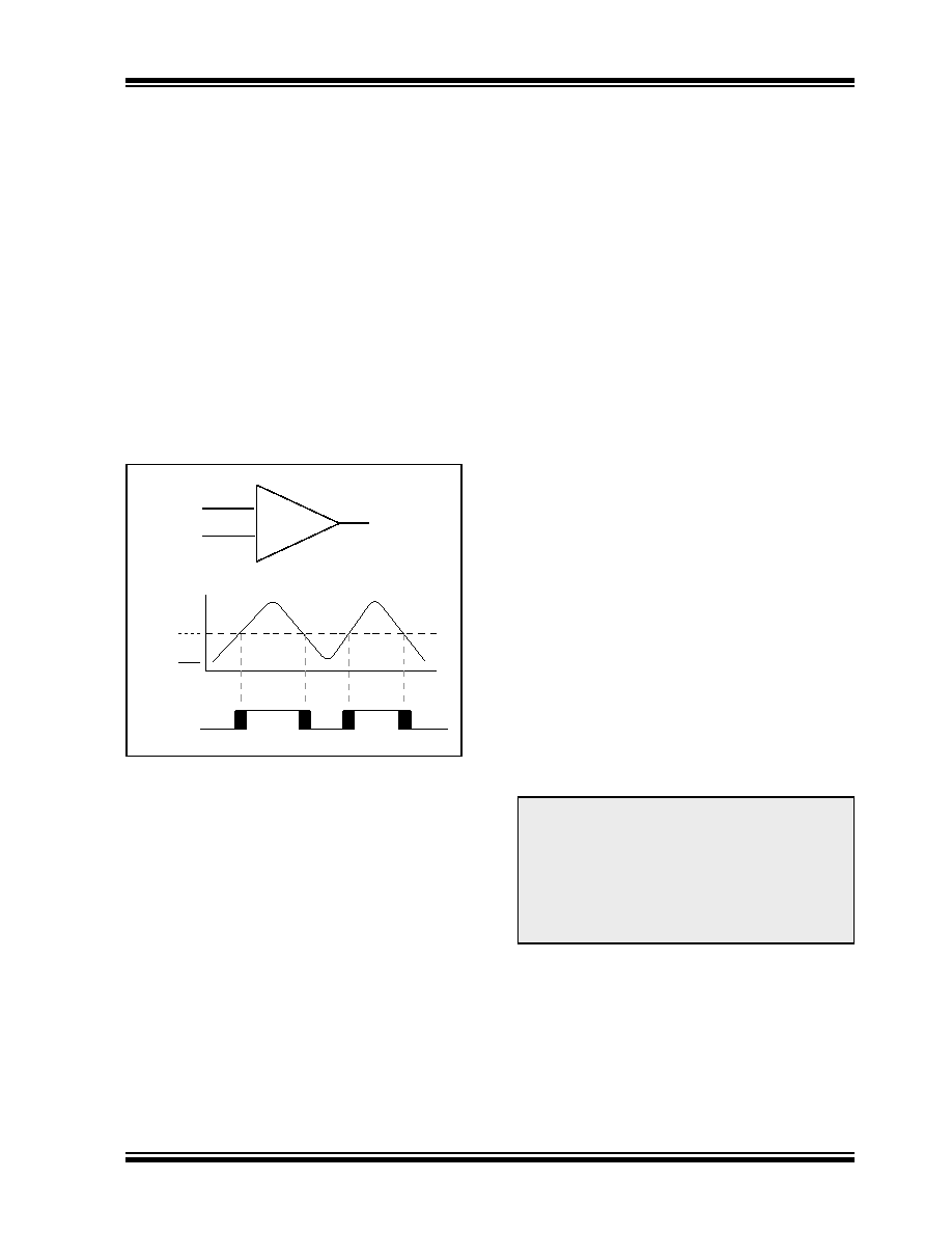
A single comparator is shown in Figure 20-2, along with
the relationship between the analog input levels and
the digital output. When the analog input at VIN+ is less
than the analog input VIN-, the output of the comparator
is a digital low level. When the analog input at VIN+ is
greater than the analog input VIN-, the output of the
comparator is a digital high level. The shaded areas of
the output of the comparator in Figure 20-2 represent
the uncertainty due to input offsets and response time.
20.3
Comparator Reference
An external or internal reference signal may be used
depending on the Comparator Operating mode. The
analog signal present at VIN- is compared to the signal
at VIN+ and the digital output of the comparator is
adjusted accordingly (Figure 20-2).
FIGURE 20-2:
SINGLE COMPARATOR
20.3.1
EXTERNAL REFERENCE SIGNAL
When external voltage references are used, the
comparator module can be configured to have the com-
parators operate from the same or different reference
sources. However, threshold detector applications may
require the same reference. The reference signal must
be between VSS and VDD and can be applied to either
pin of the comparator(s).
20.3.2
INTERNAL REFERENCE SIGNAL
The comparator module also allows the selection of an
internally generated voltage reference for the compara-
Module” contains a detailed description of the compar-
ator voltage reference module that provides this signal.
The internal reference signal is used when comparators
are in mode CM<2:0> = 110 (Figure 20-1). In this mode,
the internal voltage reference is applied to the VIN+ pin
of both comparators.
20.4
Comparator Response Time
Response time is the minimum time, after selecting a
new reference voltage or input source, before the
comparator output has a valid level. If the internal
reference is changed, the maximum delay of the inter-
nal voltage reference must be considered when using
the comparator outputs. Otherwise, the maximum
delay of the comparators should be used (Section 27.0
20.5
Comparator Outputs
The comparator outputs are read through the CMCON
register. These bits are read-only. The comparator
outputs may also be directly output to the RF1 and RF2
I/O pins. When enabled, multiplexors in the output path
of the RF1 and RF2 pins will switch and the output of
each pin will be the unsynchronized output of the com-
parator. The uncertainty of each of the comparators is
related to the input offset voltage and the response time
given in the specifications. Figure 20-3 shows the
comparator output block diagram.
The TRISA bits will still function as an output
enable/disable for the RF1 and RF2 pins while in this
mode.
The polarity of the comparator outputs can be changed
using the C2INV and C1INV bits (CMCON<4:5>).
–
+
VIN+
VIN-
Output
VIN–
VIN+
Output
VIN+
VIN-
Note 1: When reading the Port register, all pins
configured as analog inputs will read as a
‘0’. Pins configured as digital inputs will
convert an analog input according to the
Schmitt Trigger input specification.
2: Analog levels on any pin defined as a dig-
ital input may cause the input buffer to
consume more current than is specified.
发布紧急采购,3分钟左右您将得到回复。
相关PDF资料
XF2J-2424-11
CONN FPC 24POS 0.5MM SMT
PIC18LF6585T-I/PT
IC PIC MCU FLASH 24KX16 64TQFP
PIC18LF6680T-I/PT
IC PIC MCU FLASH 32KX16 64TQFP
XF2J-2224-11
CONN FPC 22POS 0.5MM SMT
PIC18F6525T-I/PT
IC PIC MCU FLASH 24KX16 64TQFP
PIC18F4439-E/ML
IC PIC MCU FLASH 6KX16 44QFN
XF2J-2024-11
CONN FPC 20POS 0.5MM SMT
PIC16LF747-I/ML
IC PIC MCU FLASH 4KX14 44QFN
相关代理商/技术参数
PIC18F85J10-I/PT
功能描述:8位微控制器 -MCU 32 KB FL 2 KB RAM RoHS:否 制造商:Silicon Labs 核心:8051 处理器系列:C8051F39x 数据总线宽度:8 bit 最大时钟频率:50 MHz 程序存储器大小:16 KB 数据 RAM 大小:1 KB 片上 ADC:Yes 工作电源电压:1.8 V to 3.6 V 工作温度范围:- 40 C to + 105 C 封装 / 箱体:QFN-20 安装风格:SMD/SMT
PIC18F85J10-I/PT
制造商:Microchip Technology Inc 功能描述:IC 8BIT MCU PIC18F 40MHZ TQFP-80 制造商:Microchip Technology Inc 功能描述:IC, 8BIT MCU, PIC18F, 40MHZ, TQFP-80
PIC18F85J10T-I/PT
功能描述:8位微控制器 -MCU 32 KB FL 2 KB RAM RoHS:否 制造商:Silicon Labs 核心:8051 处理器系列:C8051F39x 数据总线宽度:8 bit 最大时钟频率:50 MHz 程序存储器大小:16 KB 数据 RAM 大小:1 KB 片上 ADC:Yes 工作电源电压:1.8 V to 3.6 V 工作温度范围:- 40 C to + 105 C 封装 / 箱体:QFN-20 安装风格:SMD/SMT
PIC18F85J11-I/PT
功能描述:8位微控制器 -MCU 32KB Flash 2048BRAM 67I/O RoHS:否 制造商:Silicon Labs 核心:8051 处理器系列:C8051F39x 数据总线宽度:8 bit 最大时钟频率:50 MHz 程序存储器大小:16 KB 数据 RAM 大小:1 KB 片上 ADC:Yes 工作电源电压:1.8 V to 3.6 V 工作温度范围:- 40 C to + 105 C 封装 / 箱体:QFN-20 安装风格:SMD/SMT
PIC18F85J11T-I/PT
功能描述:8位微控制器 -MCU 32KB Flash 2048bytes-RAM 67I/O RoHS:否 制造商:Silicon Labs 核心:8051 处理器系列:C8051F39x 数据总线宽度:8 bit 最大时钟频率:50 MHz 程序存储器大小:16 KB 数据 RAM 大小:1 KB 片上 ADC:Yes 工作电源电压:1.8 V to 3.6 V 工作温度范围:- 40 C to + 105 C 封装 / 箱体:QFN-20 安装风格:SMD/SMT
PIC18F85J15-I/PT
功能描述:8位微控制器 -MCU 48 KB FL 4 KB RAM RoHS:否 制造商:Silicon Labs 核心:8051 处理器系列:C8051F39x 数据总线宽度:8 bit 最大时钟频率:50 MHz 程序存储器大小:16 KB 数据 RAM 大小:1 KB 片上 ADC:Yes 工作电源电压:1.8 V to 3.6 V 工作温度范围:- 40 C to + 105 C 封装 / 箱体:QFN-20 安装风格:SMD/SMT
PIC18F85J15T-I/PT
功能描述:8位微控制器 -MCU 48 KB FL 4 KB RAM RoHS:否 制造商:Silicon Labs 核心:8051 处理器系列:C8051F39x 数据总线宽度:8 bit 最大时钟频率:50 MHz 程序存储器大小:16 KB 数据 RAM 大小:1 KB 片上 ADC:Yes 工作电源电压:1.8 V to 3.6 V 工作温度范围:- 40 C to + 105 C 封装 / 箱体:QFN-20 安装风格:SMD/SMT
PIC18F85J50-I/PT
功能描述:8位微控制器 -MCU 32KB Flash 3936byte RAM RoHS:否 制造商:Silicon Labs 核心:8051 处理器系列:C8051F39x 数据总线宽度:8 bit 最大时钟频率:50 MHz 程序存储器大小:16 KB 数据 RAM 大小:1 KB 片上 ADC:Yes 工作电源电压:1.8 V to 3.6 V 工作温度范围:- 40 C to + 105 C 封装 / 箱体:QFN-20 安装风格:SMD/SMT